 ❯ Gregory Abadias, University of Poitiers, France
“Real-time growth monitoring of ultrathin Ag layers for use as transparent conductive electrodes”
Gregory Abadias is Professor at the Physics Department of the University of Poitiers, France. He received his Ph.D. degree in materials science in 1998 at National Polytechnic Institute of Grenoble (INPG), and he is currently group leader of thin films activities at CNRS Pprime Institute (https://pprime.fr/en/home-pprime/) in Poitiers. He conducts research on a range of topics related to nanoscale thin films, including mechanical, electrical and optical properties of metallic, nitride or oxide systems as well as hard and protective coatings in the form of nanocomposites or multilayers. His current research interests focus on the understanding of thin film growth dynamics using real-time and in situ diagnostics as well as computational modelling, with main emphasis on growth manipulation strategies to control morphology and stress development in sputter-deposited metal layers. He is co-authors of more than 160 papers in peer-review journals and one book chapter on stress in PVD thin films. He was member-elected to the Scientific Council of the Physics Institute of CNRS (2019-23), as well as French representative of the Surface Engineering Division of IUVSTA for 2022-25 triennium. He has been involved in the organization of several symposia or workshops at international conferences (ICMCTF, EMRS) and serves as Editor of Surface and Coatings Technology journal since 2016.
Real-time growth monitoring of ultrathin Ag layers for use as transparent conductive electrodes
Gregory Abadias
University of Poitiers, France
Noble-metal layers, with nominal thickness ~10 nm or below, are ubiquitous in a wide range of plasmonic devices and other optoelectronic applications. Silver (Ag) is by far the material of choice for a number of key technological areas, such as in smart windows for architectural glazing, selective infrared thermal emitters for radiative cooling or transparent conductive electrodes (TCEs) for flexible photovoltaics or flat panel displays. However, the growth of Ag on weakly interacting substrates (e.g. oxides) proceeds in a 3D fashion. At present, there is much interest in producing ultrathin Ag layers as potential TCE alternative to indium tin oxide, which suffers from high cost, poor sustainability, and is prone to cracking upon bending. Strategies to produce fully continuous, ultrathin and ultra-smooth Ag layers without compromising their electrical conductivity have lately been deployed. Among them, the use of gaseous additives, such as N2 or O2, or template layers appears to be an efficient route to improve Ag wetting and favor a 2D growth morphology [1-3]. However, understanding the entire evolutionary growth regime requires the implementation of in situ and real-time diagnostics.
In the present work, the impact of N2 or Ge addition on the morphological and structural evolution of ultrathin Ag layers is investigated by coupling complementary in situ and real-time diagnostics. Lab-scale studies include wafer curvature, surface differential reflectance spectroscopy and electrical resistivity to determine morphological transition thicknesses such as percolation threshold and onset of continuous film formation [4]. These results are further comprehended using real-time X-ray synchrotron studies (SIXS beamline at SOLEIL) in which the grazing incidence diffraction and small-angle scattering signals are simultaneously recorded, together with stress evolution. This enables us to explore the influence of Ge and N2 on island shape, texture and stress development, as well as relaxation mechanisms during growth interruptions.
In the case of Ag/N2 system, we additionally compared the growth morphology of Ag layers obtained by evaporation (e-beam) and sputter-deposition (dcMS and Hipims) processes. These deposition methods enabled us to span a wide range of growth conditions with respect to energies of film-forming and plasma species, as well as N2 dissociation rates, with the aim to obtain a mechanistic interpretation of the role of nitrogen.
References
[1] Jamnig, A. et al., ACS Appl. Nano Mater. 3 (2020) 4728
[2] Jeong, E. et al., Applied Surface Science 528 (2020) 146589
[3] Zapata, R. et al., ACS Appl. Mater. Interfaces 15 (2023) 36951
[4] Colin, J. et al., Nanomaterials 10, 2225 (2020)
 ❯ André Anders, Leibniz Institute of Surface Engineering (IOM), Leipzig, Germany
“Atomic scale heating in plasma deposition processes”
André Anders has a joint appointment as the Director and CEO (Direktor und Vorstand) of the Leibniz Institute of Surface Engineering, Leipzig, Germany, and Professor of Applied Physics at the Felix Bloch Institute of Solid State Physics, Leipzig University. He assumed these positions in 2017 after working at Lawrence Berkeley National Laboratory in Berkeley, CA, USA, since 1992, where he still is a Scientist Affiliate. He studied physics in Wroclaw, Poland, Berlin, (East) Germany, and Moscow (Russia, then Soviet Union), to obtain his PhD degree from Humboldt University in Berlin in 1987. André has worked for about 35 years in basic and applied plasma physics and materials sciences. He has authored 3 books and more than 350 peer-reviewed journal papers (h-index 75, over 21,000 citations, Google Scholar 2023). His work was recognized by several awards and election to Fellow level of professional societies including APS, AVS, IEEE, and IoP. Since 2014 he is the Editor-in-Chief of Journal of Applied Physics published by AIP Publishing, Melville, NY.
Atomic scale heating in plasma deposition processes
André Anders et al.
1Leibniz Institute of Surface Engineering (IOM), Permoserstr. 15, 04318 Leipzig, Germany
2Felix Bloch Institute of Solid State Physics, Leipzig University, Linnéstr. 5, 04103 Leipzig, Germany
Deposition from the plasma phase implies the supply of energy to the growing film, namely, each of the condensing atoms and ions brings kinetic and potential energy to exactly the surface locations where the film grows. This is especially effective if growth occurs by the supply of multiply charged ions. In this contribution, the concept of atomic scale heating is explained and illustrated for the case of (V, Al)N films.
 ❯ Sandra Carvalho, University of Coimbra, Portugal
“Advancing biomedical applications through plasma surface modification: A promising frontier”
Sandra Carvalho is Full Professor at the University of Coimbra (UC). She obtained her PhD in Physics in 2004, with a work carried out in Portugal, France, the Netherlands and Germany, in the field of hard PVD coatings.
After PhD, her scientific activity has been focused on the development of coatings and thin films, as well as surface treatment to enhance the performance of various components. In this regard, she leads a Surface Modification and Functionalization group (http://orcid.org/0000-0002-3643-4973).
Sandra is the scientific coordinator at UC of three Mobilizing Agendas for Business Innovation within the scope of the PRR – Portuguese Recovery and Resilience Facility launched by the European Commission, involving more than 100 members (88 companies and 15 R&D institutions and 5 associations) and an investment for UC of €7 million.
Sandra is member of the European Joint Committee on Plasma and Ion Surface Engineering and member of the Executive Committee of Advanced Surface Engineering Division of the American Vacuum Society (AVS). She is President of the Portuguese Materials Society (SPM) since 2023. Sandra serves as vice-director of the FCTUC, with responsibilities in Research, Innovation, and Knowledge Transfer.
Advancing Biomedical Applications through Plasma Surface Modification: A Promising Frontier
S. Carvalho
CEMMPRE, Department of Mechanical Engineering, University of Coimbra, Portugal
Significant advances have been made in the technology of biomedical coatings and materials. This talk will provide an extensive review of coating types and surface modifications for biomedical applications.
In many cases, side by side with traditional properties, like wear and corrosion resistance, biomaterials have to be compatible with body tissues and fluids, possess anti-microbial activity and, in specific cases, provide a good compatibility of the material with the human body (e.g. osseointegration). It is difficult to find a unique material with all these functionalities, reinforcing the importance of surface engineering to supply new functionalities. The topic of this talk is centred on surface modification of materials, traditionally used for biomedical applications, in order to improve their performance for specific cases. Different surface modification methods will be presented and potential applications such as orthopaedic, cardiovascular and urethral stents, biosensors, and dental implants will be discussed. Several case studies of antimicrobial coatings and bioactive surfaces will be presented as well.
 ❯ Grzegorz (Greg) Greczynski, Linköping University, Sweden
“Towards reliable X-ray photoelectron spectroscopy of thin films”
Grzegorz (Greg) Greczynski is a Professor in the Department of Physics, Linköping University (LiU) and the head of the Fundamental Science of Thin Films Group. Greczynski received his PhD degree in surface science of organic materials in 2001 and has an eight-year industrial track record. In 2018 he was nominated Fellow of the American Vacuum Society for “seminal contributions to nondestructive X-ray photoelectron spectroscopy (XPS) surface analysis, and the development of novel next-generation HiPIMS metal-ion deposition techniques”. His research interests are presently focused on low-energy ion/surface interactions (including both gas and metal ions) for nanostructure control during low-temperature growth of transition-metal-based nitride, boride, and carbide thin films by physical vapor deposition. Greczynski is also active in the field of XPS, with the aim to enhance the reliability of the technique. He has published 175 peer-reviewed articles that have been cited more than 10000 times.
Towards reliable X-ray photoelectron spectroscopy of thin films
G. Greczynski
Thin Film Physics Division, Department of Physics (IFM), Linköping University, SE-581 83 Linköping, Sweden
grzegorz.greczynski@liu.se; (+46 13 281213)
Raising concern within the surface science community about decreasing quality of X-ray photoelectron spectroscopy papers,i motivates efforts that would lead to an improved reliability of reported results. One of the major issues is related to an unreliable charge referencing of the binding energy scale.ii,iii Experiments conducted in our laboratory on large sets of thin film samples demonstrated spectacular failure of commonly used referencing methods based on the C 1s peak of adventitious carbonii,iv and the Ar 2p peak of implanted Ar.v When applied, both techniques generate a large spread in reported binding energy values that often exceed involved chemical shifts. Based on the model experiments, preformed on alumina layers, that can be repeated for all sorts of thin film insulators, a solution to the binding energy reference problem is proposed for reliable assessment of chemical bonding. Examples illustrating the above issues along with best practices will be discussed during the talk.
_________________
iG.H. Major, T. G. Avval, B. Moeini, G. Pinto, D. Shah, V. Jain, et al. J. Vac. Sci. Technol. A 38, 061204 (2020)
iiG. Greczynski and L. Hultman, Angew. Chem. Int. Ed. 59 (2020) 5002
iiiG. Greczynski and L. Hultman, Progress in Materials Science 107 (2020) 100591
ivG. Greczynski, O.V. Pshyk, and L. Hultman, Science Advances 9 (2023) eadi3192
vG. Greczynski and L. Hultman, Applied Surface Science 635 (2023) 157598
 ❯ Christoph Herrmann, Technische Universität Braunschweig and Fraunhofer Institute for Surface Engineering and Thin Films IST, Germany
“Holistic life cycle engineering for a sustainable circular economy”
Prof. Dr.-Ing. Christoph Herrmann is university professor for Sustainable Manufacturing & Life Cycle Engineering and co-director of IWF, Institute of Machine Tools and Production Technology, Technische Universität Braunschweig as well as director of the Fraunhofer Institute for Surface Engineering and Thin Films IST.
Holistic life cycle engineering for a sustainable circular economy
Christoph Herrmann
Technische Universität Braunschweig and Fraunhofer Institute for Surface Engineering and Thin Films IST, Germany
Despite significant improvements in the eco-efficiency of individual products and processes, the global environment has witnessed a staggering rise in pollution. To ensure a sustainable future in engineering, it is imperative to align micro-level engineering decisions with macro-level sustainability principles, like the concept of planetary boundaries that recognize the finite capacity of the Earth’s climate and ecosystems. This presentation will introduce a methodical approach that aids in pinpointing and prioritizing mitigation strategies as valuable input for life cycle engineering endeavours. Case studies within the field of surface engineering will be showcased to illustrate the practical application of this approach.
 ❯ Jyh-Wei Lee, Ming Chi University of Technology (MCUT), Taiwan
“Effect of carbon on the microstructure and properties of TiZrNbTaFeC high entropy alloy carbide coatings”
Jyh-Wei Lee is a Distinguished Professor at the Department of Materials Engineering at the Ming Chi University of Technology (MCUT), Taiwan, and a Joint Appointment Professor, at the Department of Mechanical Engineering at Chang Gung University, Taiwan. He has been the Director of the Center for Plasma and Thin Film Technologies (CPTFT) since 2021 and the Director of the International Ph.D. Program in Plasma and Thin Film Technology, MCUT, since 2023. Prof. Lee is the Chair of the AVS-Taiwan Chapter and a member of the Editorial Board of Surface & Coatings Technology, Applied Surface Science Advances, and China Surface Engineering. He is the AVS ASED Program Committee member. Prof. Lee is the Program Chair of ICMCTF2023 and General Chair of ICMCTF2024. He also serves as an International Program Committee Member, Symposium Chair, and Session Chair of several International Conferences, such as ICMCTF2015-2019, AEPSE2017-2023, ISSP2019, TACT2015-2023, PSE2022, PSE2024, etc. He was the 10th President of the Taiwan Association for Coating and Thin Film Technology (TACT), Taiwan from 2018 to 2019. Prof. Lee was the Dean of the College of Engineering, Tungnan University (TNU), Taiwan, from 2007 to 2010, and Director of the Research Center for Micro/Nanotechnologies, TNU, from 2005 to 2010.
His research focuses on developing plasma-based thin film technologies to enhance the properties and performance of functional thin films and coatings used for cutting tools, molding dies, surgical instruments, optical, antibacterial, and pollution treatments. He also investigates the nanocomposite and nanolaminated nitride, carbonitride and boronitride hard coatings for tribological applications, corrosion, and oxidation protection in related industries. Recently, he has worked on the research and development of high entropy alloy thin films and thin film metallic glass materials, which can be applied in the corrosion resistance, high-temperature, and biomedical fields. Prof. Lee is skilled in high power impulse magnetron sputtering (HIPIMS), pulsed DC magnetron sputtering, cathodic arc evaporation deposition and plasma electrolytic oxidation techniques, plasma diagnosis and feedback control, nanoindentation, AFM and related nanomechanical testing methods. Prof. Lee has some research on cold atmospheric plasma applications in medicine and health care. He also studied the chromizing and aluminizing processes for the Fe, Ni, and Co-based alloys to prolong their surface life at high temperatures in the past twenty years.
Prof. Lee is the PI and Co-PI of more than 30 projects from the Taiwan government and industries, with a total budget of around 7.0 million US$ in the past four years. He holds 13 patents and has published 205 SCI journal papers and over 30 keynote/invited lectures in the field of PVD and related surface engineering technologies. The H-index of his published paper is 42. He is also listed in the World’s Top 2% Scientists published by Stanford University from 2020 to 2022.
Effect of carbon on the microstructure and properties of TiZrNbTaFeC high entropy alloy carbide coatings
Jyh-Wei Lee 1,2,3,4*, Ismail Rahmadtulloh1,5, Bih-Show Lou6,7, Chaur-Jeng Wang5
1Department of Materials Engineering, Ming Chi University of Technology, New Taipei, Taiwan
2Center for Plasma and Thin Film Technologies, Ming Chi University of Technology, New Taipei, Taiwan
3Department of Mechanical Engineering, Chang Gung University, Taoyuan, Taiwan
4High Entropy Materials Center, National Tsing Hua University, Hsinchu, Taiwan
5Department of Mechanical Engineering, National Taiwan University of Science and Technology, Taipei Taiwan
6Chemistry Division, Center for General Education, Chang Gung University, Taoyuan, Taiwan
7Department of Orthopaedic Surgery, New Taipei Municipal TuCheng Hospital, Chang Gung Memorial Hospital, Taiwan
*Corresponding author:jefflee@mail.mcut.edu.tw
Research on high entropy alloys [1] and multicomponent alloys [2] has brought about a new era in materials design, greatly impacting the research and development of new materials. High entropy alloys and multicomponent alloys already present very promising properties, such as high fracture resistance in cryogenic temperatures, high strength at high temperatures, good oxidation resistance, good wear and erosion resistance, etc. Coatings based on high entropy alloy and multicomponent alloy concepts have been widely explored in academia and industry. Several researchers have studied the microstructural and mechanical properties of high entropy alloy carbide coatings and confirmed their low friction, high hardness, and excellent corrosion resistance [3,4]. In this study, TiZrNbTaFeC high entropy alloy carbide (HEAC) coatings were fabricated using different acetylene (C2H2) gas flow ratios through the superimposed high power impulse magnetron sputtering (HiPIMS) and medium frequency (MF) sputtering system. The phase structure of HEAC coatings was explored by XRD and TEM. The FE-EPMA and FE-SEM were used to analyze the chemical compositions and microstructures of HEACs. The nanoindenter, scratch tester, and pin-on-disk wear tester were employed to study the hardness, adhesion, and wear resistance, respectively. The corrosion resistance of HEAC coatings was evaluated by the potentiodynamic polarization test in a 3.5% NaCl aqueous solution at room temperature. It showed that the tribological performance and corrosion resistance of TiZrNbTaFeC HEAC coatings were improved by increasing carbon contents. Effects of carbon content on the phase, microstructure, hardness, adhesion, pin-on-disk tribological performance, and corrosion resistance of TiZrNbTaFeC coatings were explored in this work.
Keywords: Superimposed HiPIMS-MF, TiZrNbTaFeC, high entropy alloy carbide coating, tribological performance, potentiodynamic polarization, corrosion.
References
[1] J.-W. Yeh, S.-K. Chen, S.-J. Lin, J.-Y. Gan, T.-S. Chin, T.-T. Shun, C.-H. Tsau, S.-Y. Chang, Adv. Eng. Mater. 6 (2004) 299–303.
[2] B. Cantor, I.T.H. Chang, P. Knight, A.J.B. Vincent, Mater. Sci. Eng. A 375-377 (2004) 213–218.
[3] G. Wang, J. Xu, Y. Chen, Y.J. Zhao, Z.H. Xie, P.R. Munroe, J. Alloys Compd. 965 (2023) 171342,
[4] M. Braic, V. Braic, M. Balaceanu, C.N. Zoita, A. Vladescu, E. Grigore, Surf. Coat. Technol. 204 (2010) 2010–2014.
 ❯ Paul H. Mayrhofer, Technical University Wien, Vienna, Austria
“High-entropy Hägg phases; A case study of nitrides, carbides, and diborides”
Paul Mayrhofer is University Professor of Materials Science at the Institute of Materials Science and Technology, and chairs the Materials Science Division at the University TU Wien, Vienna, since 2012. He received a Dr. in 2001 and habilitated in 2005 in Nanostructured Materials at the University of Leoben. In 2003, 2005, and 2006, Paul Mayrhofer spent his post-doc years and Erwin-Schrödinger-Fellowship at the University of Illinois at Urbana-Champaign, RTWH Aachen, and Linkoping University. Paul is currently Dean of Academic Affairs for Materials Science, and Mechanical and Industrial Engineering at TU Wien. Editor for Short Communications of Vacuum, and in the Editorial Board of Surface and Coatings Technology.
He has pioneered age hardening within hard ceramic thin films based on ternary nitrides and borides and is fascinated by phase transitions in general. His research activities focus on the development and characterization of vapor phase deposited nanostructured materials by a combination of computational and experimental material science. He won the prestigious START price of the Austrian Science Fund and served scientific societies in numerous appointed and elected positions. Paul is an elected member of the Austrian Academy of Sciences. He is active in the ASED, where he has served as Division Chair in 2020. He was Editor of the ICMCTF Proceedings in the years 2007, 2008 and 2009, and the Program and General Chair of ICMCTF in 2012 and 2013. He also served as the Chair of the ASED Sessions at the AVS International Symposium and Exhibition (2008–11, 2016–17). Paul is Fellow of AVS for Seminal contributions in the development of vapor phase deposited nanostructured materials and self-hardened protective coatings of ternary nitrides and borides. He has published more than 310 SCI listed papers in the general field of thin film materials science, with >16,500 citations to these (h-index of 69; GS) and holds 13 patents regarding hard coatings.
High-entropy Hägg phases; A case study of nitrides, carbides, and diborides
Paul H. Mayrhofer
Institute of Materials Science and Technology, TU Wien, 1060 Vienna, Austria, paul.mayrhofer@tuwien.ac.at
So-called high-entropy materials often outperform their lower-entropy relatives in various aspects. Compared to metallic high-entropy alloys, little is known for high-entropy intermetallics, such as the Hägg phases (which include the nitrides, carbides, and diborides of the transition metals). The term “high-entropy” is often used also for this type of materials if they consist of at least five binaries and the configurational entropy (per formula unit) is S ≥ 1.5R. Since such intermetallics usually consist of two sublattices, one of which is essentially unchanged, the term “high-entropy metal sublattice nitrides”, carbides, borides, etc. seems more appropriate and precise. Detailed experimental and computational studies show that single-phased materials of this type can exhibit exceptional strength, thermal stability, and oxidation resistance. Furthermore, all magnetron sputtered thin films with a high-entropy metal sublattice investigated were relatively insensitive to variations in their deposition parameters.
❯ Carmen Menoni, Colorado State University, CO, USA
“Amorphous oxides mixtures for coatings of gravitational wave detectors”
Dr. Carmen S. Menoni is University Distinguished Professor in the Department of Electrical and Computer Engineering. She also holds appointments in the department of Chemistry, and the School of Advanced Materials Discovery. Prof. Menoni’s group investigates the synthesis of amorphous thin film oxides by sputtering and uses spectroscopic and other material diagnostics to identify their structural organization at the nanoscale. Through a combination of fundamental understanding of the optical and structural properties of the thin film materials and device engineering, Prof. Menoni research is advancing the state-of-art in interference coatings for gravitational wave detectors and ultra-high intensity lasers. Prof. Menoni is Fellow of the Institute of Electrical & Electronic Engineers (IEEE), the American Physical Society (APS), the Optical Society of America (OSA), the American Association for the Advancement of Science (AAAS) and the International Society for Optics and Photonics (SPIE).
Amorphous oxides mixtures for coatings of gravitational wave detectors
Carmen S. Menoni1, Aaron Davenport2, Samuel Castro-Lucas2, Ruth Osovsky-Shpilman2, Sangita Bhowmick2, Ashot Markosyan3, Riccardo Bassiri3, Martin Fejer3, François Schiettekatte4, Martin Chicoine4, Rui Zhang5, Jun Jiang5, Hai-Ping Cheng5
1Department of Electrical and Computer Engineering, Colorado State University, Fort Collins, CO, USA
2Department of Electrical and Computer Engineering, Colorado State University, Fort Collins, CO, USA
3Gintzon Lab, Stanford University, Stanford, CA, USA
4Department of Physics, University of Montreal, Quebec, Canada
5Department of Physics, Northeastern University, Boston, MA, USA
The mixing of two or more cations in the ion beam sputtering (IBS) of amorphous oxides provides enormous flexibility to tailor the optical and mechanical properties of the mixture thin films. Cation mixing has been instrumental in coatings for gravitational wave detectors to achieve the lowest possible coating thermal noise. Using as example mixtures of TiO2 and GeO2 with Ti content ranging from 0 to 60%, this talk will describe the modifications in the atomic structure and bonding that occur when Ti is added to amorphous GeO2. It will be shown that for a Ti content of up to about 44%, the Ti ions substitute Ge ions in the network forming Ti-O-Ge bonds which are mainly corner-shared. Annealing also promotes this type of structural rearrangement, more significantly at temperatures ≥ 500°C and before the onset of crystallization. This type of network organization is paramount to reduce internal friction, as demonstrated in IBS mixtures of 44% TiO2 and 56% GeO2 coatings which have achieved a value of internal friction ~4x lower than state-of-the art 25% TiO2:Ta2O5 used for coatings of gravitational wave detectors. This work brings out a new understanding of the modifications in the atomic structure of TiO2:GeO2 mixtures with composition and upon thermal treatment, which is critical to understand the mechanisms involved in affecting internal friction.
 ❯ Ivan Petrov, Linköping University, Sweden
“Low-temperature synthesis of dense, hard, stress-free ceramic coatings using metal-ion irradiation”
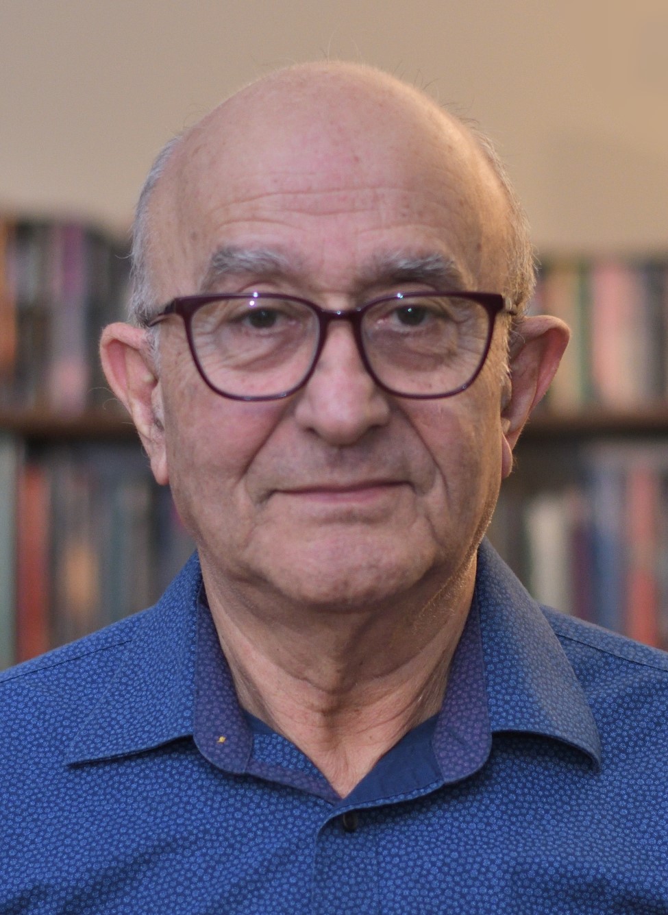
Ivan Petrov is a Professor of Physics at Linköping University, Sweden. He was a Professor of Materials Science and Principal Research Scientist at the Materials Research Laboratory (1998-2010), and Director of the Center for Microanalysis of Materials at the University of Illinois. Ivan earned his Ph.D. in Physics from the Bulgarian Academy of Sciences and received a Doctor Honoris Causa Degree from Linköping University, Sweden. He has published over 350 refereed papers cited > 22 000 times with H-index of 77. Ivan is an Editor of Surface and Coatings Technology. He is a Fellow and Honorary Member of AVS and received the 2009 Bunshah Award from the ASED, and the 2013 AVS John Thornton award “for his seminal contributions in determining the role of low-energy ion/surface interactions for controlling microstructure evolution during low-temperature growth of transition-metal nitride layers.” In 2017 he received the Lifetime Achievement Award from the Taiwan Association for Coatings and Thin Film Technology. He has been elected as Chair of the Surface Engineering Division of IUVSTA 2007-2022.
Low-temperature synthesis of dense, hard, stress-free ceramic coatings using metal-ion irradiation
Ivan Petrov1,2,*, Lars Hultman1, Joe Greene1,2 and Greg Greczynski1
1Thin Film Physics Division, Department of Physics (IFM), Linköping University, SE-581 83 Linköping, Sweden
2Materials Research Laboratory, University of Illinois, Urbana, Illinois 61801
*Corresponding author: petrov@illinois.edu
Ion irradiation is a key tool for controlling epitaxy-to-nanostructure, phase content, and physical properties of refractory ceramic thin films grown by magnetron sputtering. Until recently, thin film growth relied on enhancing adatom mobility in the surface region by inert and/or reactive gas ion irradiation to obtain dense layers at low deposition temperatures. Development of high-power pulsed magnetron sputtering (HiPIMS), which provides metal-ion plasmas with tunable degree of ionization, enabled systematic studies of the effects of metal-ion irradiation on properties of refractory ceramic thin films. A motivation for the use of metal-ions stems is that they are film constituents, hence they can provide the benefits of ion-mixing without causing the high compressive stresses associated with trapping of gas ions at interstitial sites.
This presentation reviews growth experiments of transition metal nitride model systems including TiAlN, TiSiN, VAlN, TiTaN, TiAlTaN, and TiAlWN.1 Film synthesis is carried out in a hybrid configuration with one target powered by HiPIMS and other operated in direct current magnetron sputtering (DCMS) mode. A substrate bias potential Vs is synchronized with the metal-ion-rich portion of the HiPIMS pulses to control the metal-ion energy. The time-resolved mass spectrometry analyses performed at the substrate position enables us to suppress the role of gas ion irradiation and select intense M1n+ and M2n+ metal-ion fluxes (n = 1, 2) to study the effects on film growth kinetics over a wide range of M1M2N alloy compositions. We establish new and quite different pathways for nanostructure control when using either light or heavy metal ions.
Irradiation with lower-mass metal-ions (Al+ or Si+) results in near-surface implantation with the depth controlled by Vs amplitude. This enables synthesis of metastable ternary cubic Me1Me2N solid solutions far above the Me1N concentration range achieved by DCMS.2 At the other extreme, bombardment of the growing film surface with pulsed high-mass metal ion fluxes (W+ or Ta+)3 during hybrid HiPIMS/DCMS high-rate deposition of dilute Ti1-xTaxN, Ti1-x–yAlxTayN, and Ti1-x–yAlxWyN alloys provides high fluxes of low energy recoils and results in fully-dense, low-stress, hard and superhard coatings without external substrate heating (temperature ≤ 130 °C). In addition to energy savings, this approach dramatically expands the application of such coatings on temperature sensitive substrate.
For cubic-TiAlWN, we recently discovered that Guinier-Preston (GP) zone hardening – previous known from soft light-metal alloys – can operate in a refractory ceramic.4 The present GP hardening at 1000 °C is by the formation of atomic-plane-thick W populating {111} planes.
References
1G. Greczynski, I. Petrov, J.E. Greene, and L. Hultman, J. Vac. Sci. Technol. A 37 (2019) 060801
2G. Greczynski, S. Mráz, J.M. Schneider, L. Hultman, J. Appl. Phys. 127 (2020) 180901
3G. Greczynski, L. Hultman I. Petrov, J. Appl. Phys. 123 (2023) 140901
4O. Pshyk, X. Li, I. Petrov, D.G. Sangiovanni, J. Palisaitis, L. Hultman, G. Greczynski, Mater Des 227(2023) 111753
 ❯ Stephan Reuter, Polytechnique Montréal, Quebec, Canada
“Advanced laser diagnostics on reactive plasmas at interfaces”
Stephan Reuter is full professor for plasma physics and spectroscopy at the Engineering Physics Department of Polytechnique Montréal and TransMedTech chair for plasma medicine. Following his PhD at University Duisburg-Essen in Germany, he first was research fellow at the center for plasma physics at Queen’s University Belfast, UK and then established and led the “plasmatis” physics research group for plasma medicine at the Leibniz Institute INP Greifswald, Germany. From 2017 to 2018, he was Feodor-Lynen Fellow at Princeton University. He is alumnus of the Alexander von Humboldt Foundation.
Advanced laser diagnostics on reactive plasmas at interfaces
Stephan Reuter,
Polytechnique Montréal, Quebec, Canada
Non-thermal atmospheric pressure plasmas provide high reactivity at low gas temperatures, making them ideal for coating and functionalization of thermally sensitive surfaces. Focus is currently on cold plasma jets and their potential for plasma-based surface functionalization in industrial and medical applications [1]. By adding precursors to the plasma jet feed gas, functional coatings and surface modifications are created. To achieve desired surface properties of plasma-treated substrates, more detailed knowledge of the plasma processes is needed. The presentation discusses state of the art optical diagnostics for the characterization of plasma jets’ reactive species, as well as electric and flow fields [2-4]. Highlighted are the advantages and challenges of ultrafast time resolved laser spectroscopy in combination with electrical diagnostics of cold reactive plasma jets.
References
[1] Booth, J.-P., Mozetič, M., Nikiforov, A. & Oehr, C., 2022. Foundations of plasma surface functionalization of polymers for industrial and biological applications. PSST 31 103001.
[2] Schäfer, J., Foest, R., Reuter, S., Kewitz, T., Sperka, J. & Weltmann, K. D., 2012. Laser schlieren deflectometry for temperature analysis of filamentary non-thermal atmospheric pressure plasma. Rev Sci Instrum, 83, 103506.
[3] Reuter, S., Winter, J., Schmidt-Bleker, A., Schroeder, D., Lange, H., Knake, N., Schulz-Von Der Gathen, V. & Weltmann, K. D., 2012. Atomic oxygen in a cold argon plasma jet: TALIF spectroscopy in ambient air with modelling and measurements of ambient species diffusion. Plasma Sources Science & Technology, 21, 024005.
[4] Hogue, J., Cusson, P., Meunier, M., Seletskiy, D. V. & Reuter, S., 2023. Sensitive detection of electric field-induced second harmonic signals. Opt Lett, 48, 4601-4604.
 ❯ Jochen M. Schneider, RWTH Aachen University, Germany
“Thin film materials design & some thoughts on complexity and sustainability”
Jochen M. Schneider, Ph.D., is Professor of Materials Chemistry at RWTH Aachen University, Germany. His research focus is quantum-mechanically guided design of thin films regarding thermal and chemical stability as well as elasticity. He also designs self-reporting materials.
Jochen has been awarded the Sofya Kovalevskaya Prize by the Alexander von Humboldt Foundation for excellence in thin film materials science research in 2001 and was named a Fellow of American Vacuum Society (AVS) in 2013. In 2015 he was appointed as Max Planck Fellow. Also, in 2015 Jochen was named RWTH Fellow. In 2020 he was the Bill Sproul Award and Honorary ICMCTF Lecture Recipient. In 2022 received the Rudolf-Jaeckel-award of the German Vacuum Society to recognize outstanding achievements in vacuum-based sciences. In 2023 he was appointed as Honorary doctor of the Faculty of Science and Technology, Uppsala University, Sweden.
Thin film materials design & some thoughts on complexity and sustainability
Jochen M. Schneider
Materials Chemistry, RWTH Aachen University, Germany
Designing the next generation of thermally and chemically stable thin films without utilizing trial and error-based methodologies requires truly predictive computational approaches. Important design criteria for protective thin film materials are, besides phase formation, mechanical behavior as well as thermal – and chemical stability. Examples of predictions thereof showcasing so-called MAB phases [1], transition metal nitrides [2], and transition metal aluminum nitrides [3] and transition metal aluminum diborides [5] which are chemically modified will be presented. Furthermore, the generation of point defects in transition metal aluminum nitrides by ion bombardment is predicted [5,6]. All aforementioned predictions are critically appraised by experimental data. Implications for future design efforts will be discussed also in the context of (chemical and structural) complexity as well as sustainability.
References
[1] D. Bogdanovski, P.J. Pöllmann, J.M. Schneider, An ab initio investigation of the temperature-dependent energetic barriers towards CrAlB and (Mo,Cr)AlB formation in a metastable synthesis scenario; Nanoscale 10(35), 12866-12874 (2022), [doi.org/10.1039/D2NR01087A]
[2] P. Ondračka, M. Hans, D. Holzapfel, D. Primetzhofer, D. Holec, J. M. Schneider, Ab initio-guided X-ray photoelectron spectroscopy quantification of Ti vacancies in Ti1−δOxN1−x thin films; Acta materialia 230, 117778 (2022), [doi.org/10.1016/j.actamat.2022.117778]
[3] D. M. Holzapfel, D. Music, M. Hans, S. Woof-Goodrich, D. Holec, D. Bogdanovski, M. Arndt, A. O. Eriksson, K. Yalamanchili, D. Primetzhofer, C. H. Liebscher, J. M. Schneider, Enhanced thermal stability of (Ti,Al)N coatings by oxygen incorporation, Acta Materialia 218, 117204 (2021), [doi.org/10.1016/j.actamat.2021.117204]
[4] A. H. Navidi Kashani, S. Mráz, D. Holzapfel, M. Hans, L. Löfler, P. Ondračka, D. Primetzhofer, J. M. Schneider, Synthesis and oxidation behavior of Ti0.35Al0.65By (y = 1.7–2.4) coatings, Surface and coatings technology 442, 128190 (2022), [doi.org/10.1016/j.surfcoat.2022.128190]
[5] S. Karimi Aghda, D. Music, Y. Unutulmazsoy, H.H. Sua, S. Mráz, M. Hans, D. Primetzhofer, A. Anders, J.M. Schneider, Unravelling the ion-energy-dependent structure evolution and its implications for the elastic properties of (V,Al)N thin films, Acta Materialia 214, 117003 (2021), [doi.org/10.1016/j.actamat.2021.117003]
[6] D. Holzapfel, D. Music, S. Mráz, S. Aghda, M. Etter, P. Ondračka, M. Hans, D. Bogdanovski, S. Evertz, L. Patterer, P. Schmidt, A. Schökel, A. O.Eriksson, M. Arndt, D. Primetzhofer, J. Schneider, Influence of ion irradiation-induced defects on phase formation and thermal stability of Ti0.27Al0.21N0.52 coatings, Acta Materialia 237, 118160 (2022), [doi.org/10.1016/j.actamat.2022.118160]
 ❯ Frederic Schuster, CEA, Paris-Saclay, France
“Thin film technologies for low carbon energies in a Green Deal context”
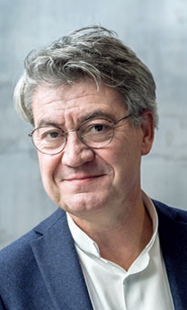
Since 2006, Frederic Schuster has been the Director of the Cross-Disciplinary Program on Material Science & Engineering at CEA. He previously held the position of deputy director of the Institute for Renewable Energies (CEA/Liten) from 2003 to 2006. In parallel, he initiated and managed the European program Nanosafe on risk management in the field of nanotechnology from 2005 to 2010 and continued to develop a multidisciplinary approach in partnership with Canada, Japan and the US on this issue. He founded the International Conference NANOSAFE (every two years in Minatec, Grenoble, since 2008) on the safe production and use of nanomaterials. He is also the founder of the IMPACT International Chair on Accelerated Discovery of Materials and Emerging Processes at the National Institute for Nuclear Science and Technology and University of Paris-Saclay. He is also the chairman of the additive manufacturing and circular economy commissions within the French Society of Metallurgy and Materials.
Since June 2022 he is co-director (with CNRS) of the French national initiative on accelerated discovery of materials, the national program DIADEM (DIscovery Acceleration for the Deployment of Emerging Materials).
Frederic Schuster is a CEA international expert in the field of materials science and engineering and especially in surface technology. For 8 years he was in charge of the CEA surface engineering laboratory at CEA Grenoble. Before his experience with CEA, he began his career in industry as manager of surface treatment department in the Arcelor-Mittal group, where he helped industrialize PVD technologies for steel surface functionalization.
Frederic Schuster is graduated from the National Polytechnic Institute of Toulouse. He received an award from the Institute in 1990 for his PhD work on MOCVD technology. He was awarded the RIST prize (young researcher) by the French Society of Metallurgy and Materials for his technology transfer achievements in the industry. In 2018, he received the Grand Award for technological innovation from the French Society for Nuclear Energy for his work on Hipims PVD coatings for Enhanced Accident Tolerant Fuels. He is the author of several patents on surface engineering, nanomaterials, and 3D printing and has published numerous articles.
Thin film technologies for low carbon energies in a Green Deal context
Frédéric Schuster
CEA, Paris-Saclay, France
The development of thin-film engineering is absolutely strategic for advanced manufacturing of components that have to operate under extreme environments (nuclear energy, renewables, aeronautics in particular). These components are often exposed to a combination of constraints, thus requiring the design of architectured systems to meet, in fine, the multi-functionality expected (diffusion barrier, resistance to oxidation and irradiation, mechanical resistance…).
Thin-film engineering is a field of technology that has made enormous progress in recent years, mainly challenged by the effective improvements demanded by the ever more uncompromising specifications of the microelectronics industry on the one hand, the booming low-carbon energies (in particular photovoltaics, hydrogen economy, as well as future of nuclear industry) and high-performance mechanics, on the other.
These advances concern PVD (Physical Vapor Deposition) technologies, in particular with the deployment of highly ionized plasma generation systems such as HiPIMS (High Power Impulse Magnetron Sputtering), which enable much better control of interface construction and coating microstructures, and, in fine, coating properties. These advances also concern CVD (Chemical Vapor Deposition) technologies, in particular thanks to the rich chemistry of organometallic compounds that can be used through the great flexibility of DLI-MOCVD (Direct Liquid Injection Metal Organic Chemical Vapor Deposition).
The field of thin films is also strongly impacted by the coupling between materials science and digital technologies, in particular artificial intelligence. On the one hand, this coupling is enabling the accelerated discovery of coatings, but it is also accelerating the mastery of sovereignty processes.
 ❯ Chris H. Stoessel, StoesselConsulting / SputterTek LLC, Palo Alto, CA, USA
“Leveraging “external innovation” to enhance the success of commercializing advances in functional coatings & surface engineering”
Chris H. Stoessel is a partner and engineering consultant at SputterTek LLC where he advises on innovation management, process engineering and product development in thin films, surface engineering and materials science. He was a Senior Process Development Manager at Eastman Chemical Co.’s Palo Alto Advanced Technology Center (formerly Southwall Technologies Inc.) in Palo Alto, California. As a member of the Corporate Innovation group, he advised on innovation strategy and managed internal and external innovation projects to develop new deposition processes and products, primarily focused on roll-to-roll coating technologies. He holds a Doctorate in Mechanical Engineering (Materials Science) from the Rheinische Westfälische Technische Hochschule Aachen (Germany), and conducted post-doctoral studies under Rointan Bunshah at UCLA. He has developed thin-film products and deposition processes for a wide range of applications such as tribology, superconducting films, optical coatings (at OCLI/JDS-Uniphase), MEMS, OLED (at DuPont Displays), energy-efficient glazing (at Southwall Technologies/Eastman Chemical Co.), and flexible hybrid electronics (FHE). Chris contributes to several professional organizations in the thin film coating community, and is the Program Director for the Society of Vacuum Coaters (SVC).
Leveraging “external innovation” to enhance the success of commercializing advances in functional coatings & surface engineering
Chris H. Stoessel
StoesselConsulting / SputterTek LLC, Palo Alto, CA, USA
Corporate implementation of advances in coating and surface science increasingly depends on effectively leveraging innovation that is obtained from external partners. External innovation offers the opportunity to reduce risks, accelerate time-to-market, nimbly react to shifting trends, diversify sources for creativity, and to take advantage of existing technology / market ecosystems. However, it can also pose challenges for corporate intellectual property strategies, stir “not invented here” resentments with internal innovation resources, requires efficient opportunity scouting, prudent due-diligence assessments, and a strategic funding and investment approach. A wholistic commitment throughout the enterprise is required to effectively integrate external innovation into corporate business structures.
In this talk, we will review various external innovation pathways, characterize their strength and weaknesses, explain how academic and tech transfer organizations can play effective “external innovation” roles, and provide guidance how to avoid common pitfalls to leverage external innovation opportunities for successful business growth in technology-driven markets such as coatings and surface engineering.
